5 years ago, I was trying to design a CCD camera for astrophotography in my spare time. But since I was major in Software Development, I didn't know much about hardware design other than 8051 MCU. After 1 year with many failures on wrong directions, I just clarified I'd better use CPLD or FPGA with Verilog/VHDL for sequential logic circuit instead of using a MCU everywhere. It was a hard progress. I had a goal too huge, and was eager for the result.
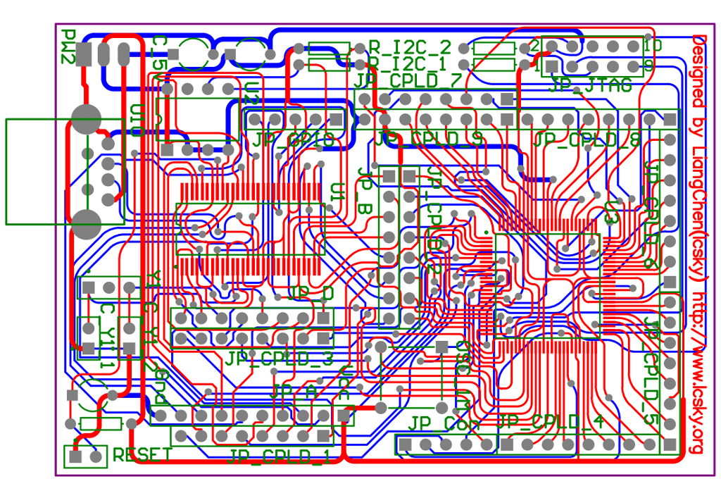
By making some tiny CPLD projects those years, I had a better understanding on sequential/combinational logic design using Verilog. I made a general experiment board for one of the projects, it mounted a Altera CPLD EPM570T100 and a Cypress 68013A USB client controller with 51 core. So I thought I can continue the camera designing now.
Last time, I was stopped by the RAM size limitation which should store a whole frame data of the Image sensor before sending via USB bulk protocol. So we begin by a little step: adding an external SDRAM to the system.
SDRAM has much complex timing diagram than SRAM. It has 6 operation stages for a simple single read: Active a "row", Wait For the "tRCD", send Read Command with a "column", PRECHARGE(means "DeActive"), Wait for the "CAS Latency", Read data.
tRCD is a const time related to the chip, my "H57V2562GTR-60C" has the tRCD equals to 18ns.
CAS Latency can be set during "Load Mode Register" stage. It can be 2 or 3 clock period.
More efficiently, there is "Brush Mode" for both reading and writing which can continuous read or write within a Active-Precharge period. But We are not going to discuss about it in this design.
I want to design a module to convert this complex interface into a more simple one. Operations which begin with a START signal on a rising-edge of the clock, need to wait for the FINISH signal only. So that a byte was read out or written into the SDRAM. The complex 6 stages would be hidden behind this module.
A FSM was created to handle this:
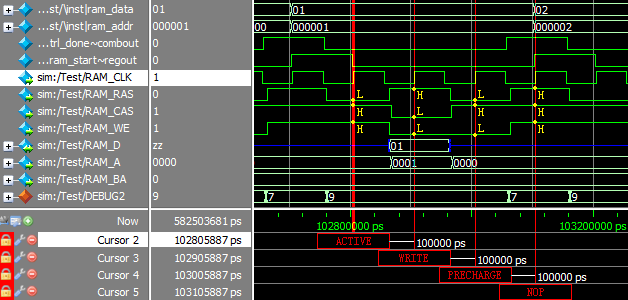
The whole write operation simulated at gate level by ModelSim(Altera Edition):
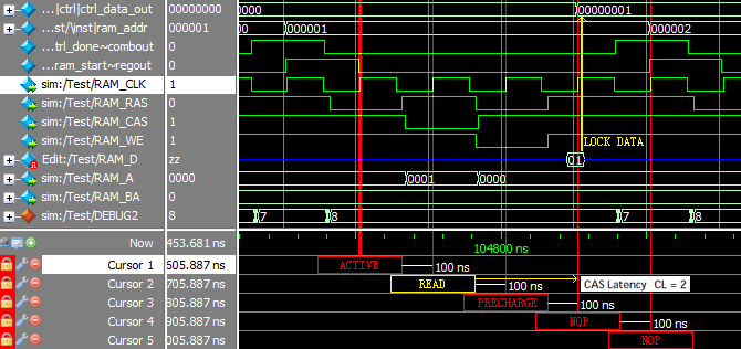
The read operation simulated at gate level:
Since I would operate the module at 10Mhz, the clock period is 100ns, the tRCD(18ns) is less than one clock time, so the NOP at T1 & T2 is not necessary.
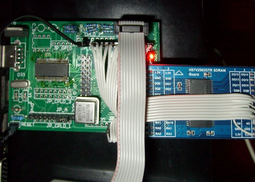
My general experiment board with the SDRAM board mounted by half DIP sockets and half "jumper wires":
Here is the code:
//Author: Lcsky.org
//Reference: http://www-inst.eecs.berkeley.edu/~cs150/fa02/handouts/10/Lab/
//Date: 2012/09/22

// Control module for SDRAM.
module sdram_ctrl (
		 RAM_D,				// to SDRAM
		 RAM_CLK,			// to SDRAM
		 RAM_DQM,			// to SDRAM
		 RAM_CS,				// to SDRAM
		 RAM_RAS,			// to SDRAM
		 RAM_CAS,			// to SDRAM
		 RAM_WE,				// to SDRAM
		 RAM_BA,				// to SDRAM
		 RAM_A,				// to SDRAM
		 CLK_IN, 			// Clock Line
		 CTRL_RESET_IN,	// Control Line
		 CTRL_START_IN,	// Control Line
		 CTRL_W_IN,			// Control Line
		 CTRL_ADDR_IN,		// Control Line
		 CTRL_DATA_IN,		// Control Line
		 CTRL_DATA_OUT,	// Control Line
		 CTRL_DONE_OUT,		// Control Line
		 DEBUG_OUT		// Control Line
	);

	inout[7:0] RAM_D;
	output RAM_CLK;
	output RAM_DQM;
	output RAM_CS;
	output RAM_RAS;
	output RAM_CAS;
	output RAM_WE;
	output[1:0] RAM_BA;
	output[12:0] RAM_A;
	input CLK_IN;
	input CTRL_RESET_IN;
	input CTRL_START_IN;
	input CTRL_W_IN;
	input[23:0] CTRL_ADDR_IN;	// 24bit address for 16M units
	input[7:0] CTRL_DATA_IN;
	output[7:0] CTRL_DATA_OUT;
	output CTRL_DONE_OUT;
	output[3:0] DEBUG_OUT;

	//Clock: 10M
	parameter[31:0] CLK_SPEED = 10000000;

	// counter for states
	wire[15:0] count;
	reg count_rst;

	// current and nextstate
	reg[3:0] CS;
	reg[3:0] NS;

	// different commands that can be issued to the SDRAM
	reg NOP;
	reg loadModeRegister;
	reg active_read, active_write;
	wire active;
	reg read;
	reg write;
	reg precharge;
	reg autoPrecharge;
	reg burstTerminate;
	reg autoRefresh;
	reg selfRefresh;
	reg data_out_lock;

	// counter for incrementing address
	reg[12:0] addr_out;
	reg[1:0] bank_addr;

	reg[23:0] ctrl_addr_in;
	reg[7:0] ctrl_data_in;
	reg[7:0] ctrl_data_out;
	reg ctrl_done;

	// mapping of commands to control lines Table1 p12 DATA sheet
	assign RAM_RAS = ~(active | precharge |
				  autoRefresh | selfRefresh
				  | loadModeRegister);
	assign RAM_CAS = ~(read | write |
				  autoRefresh | selfRefresh
				  | loadModeRegister);
	assign RAM_WE = ~(write | burstTerminate |
				 precharge | loadModeRegister);

	assign RAM_CLK = ~CLK_IN;
	assign RAM_CLKE = 1;
	assign RAM_DQM = 0;
	assign RAM_CS = 0;
	assign RAM_BA = bank_addr;
	assign RAM_A = addr_out;
	assign DEBUG_OUT = CS;

	assign active = active_write | active_read;

	assign RAM_D = write ? ctrl_data_in : 8'bzzzzzzzz;

	assign CTRL_DATA_OUT = ctrl_data_out;
	assign CTRL_DONE_OUT = ctrl_done;

	// muxing of row addr, column addr, and mode-register data
	// into to 12bit address line
	always @(ctrl_addr_in or loadModeRegister or read or write or active_read or active_write)
	begin
		if (write) begin //(addr = column addr) when reading and writting, A10=0 (no auto precharge)
			addr_out = {2'b00, 1'b0 /* A10 */, 1'b0, ctrl_addr_in[8:0]};
		end else if (read) //(addr = column addr) when reading and writting, A10=0 (no auto precharge)
			addr_out = {2'b00, 1'b0 /* A10 */, 1'b0, ctrl_addr_in[8:0]};
		else if (loadModeRegister) // mode data
			addr_out = {3'b000, 1'b1 /* Single Burst */, 2'b00, 3'b010 /* CAS Latency = 2 */, 1'b0, 3'b000};
		else if (active_write) //(addr = row addr) when active_write
			addr_out = ctrl_addr_in[21:9];
		else begin //(addr = row addr) when active_read
			addr_out = ctrl_addr_in[21:9];
		end
	end

	always@(ctrl_addr_in or active_read or active_write or read or write)
	begin
		if (active_read|read)
			bank_addr = ctrl_addr_in[23:22];
		else
			bank_addr = ctrl_addr_in[23:22];
	end

	counter #(16) state_counter(.OUT(count), .CLK(CLK_IN),
					 .ENABLE(1), .RESET(count_rst));

	parameter[3:0]
		idle = 0,
		init_wait = 1,
		init_precharge = 2,
		init_auto_refresh1 = 3,
		init_auto_refresh2 = 4,
		init_load_mode_reg = 5,
		pause_state = 7,
		read_state = 8,
		write_state = 9,
		stop_state = 10;

	always @ (posedge CLK_IN) begin
		if (CTRL_RESET_IN) begin
			CS <= idle;
		end else begin
			CS <= NS;
		end
	end

	always @ (negedge CLK_IN) begin
		if (data_out_lock && CS == read_state) begin
			ctrl_data_out <= RAM_D;
		end
	end

	always @(*) begin
		NOP = 0;
		loadModeRegister = 0;
		active_read = 0;
		active_write = 0;
		read = 0;
		write = 0;
		precharge = 0;
		autoPrecharge = 0;
		burstTerminate = 0;
		autoRefresh = 0;
		selfRefresh = 0;
		data_out_lock = 0;

		count_rst = 0;

		case (CS) /* synthesis full_case */

			idle:begin
				NS = init_wait;
				count_rst = 1;
				ctrl_done = 0;
			end

			init_wait:begin // nop for 100 micro sec
				NOP = 1;
				if (count == CLK_SPEED/10000) begin
					NS = init_precharge;
					count_rst = 1;
				end else
					NS = init_wait;
			end

			init_precharge:begin // 2 cycles (all banks): precharge, nop
				if (count == 0) begin
					precharge = 1;
					NS = init_precharge;
				end else begin
					NOP = 1;
					count_rst = 1;
					NS = init_auto_refresh1;
				end
			end

			init_auto_refresh1:begin // 8 cycles: auto-refresh, nopX7
				if (count == 0) begin
					autoRefresh = 1;
					NS = init_auto_refresh1;
				end else if (count == 7) begin
					NOP = 1;
					NS = init_auto_refresh2;
					count_rst = 1;
				end else begin
					NOP = 1;
					NS = init_auto_refresh1;
				end
			end

			init_auto_refresh2:begin // 8 cycles: auto-refresh, nopX7
				if (count == 0) begin
					autoRefresh = 1;
					NS = init_auto_refresh2;
				end else if (count == 7) begin
					NOP = 1;
					NS = init_load_mode_reg;
					count_rst = 1;
				end else begin
					NOP = 1;
					NS = init_auto_refresh2;
				end
			end

			init_load_mode_reg:begin // 2 cycles
				if (count == 0) begin
					loadModeRegister = 1;
					NS = init_load_mode_reg;
				end else begin
					NOP = 1;
					count_rst = 1;
					NS = pause_state;
				end
			end

			pause_state: begin // waiting for CTRL_START_IN
				NOP = 1;
				if (CTRL_START_IN) begin
					NS = CTRL_W_IN ? write_state : read_state;
					count_rst = 1;

				end else begin
					NS = pause_state;
					ctrl_done = 1;
				end
			end

			write_state: begin // 3 cycles: active, write, precharge
				NS = write_state;
				if (count == 0) begin
					ctrl_addr_in = CTRL_ADDR_IN;
					ctrl_data_in = CTRL_DATA_IN;
					ctrl_done = 0;

					active_write = 1;
				end else if (count == 1) begin
					write = 1;
				end else begin
					count_rst = 1;
					precharge = 1;
					NS = pause_state;
				end
			end

			read_state: begin // 4 cycles: active, read, precharge, nop(get data back)
				NS = read_state;
				if (count == 0) begin
					ctrl_addr_in = CTRL_ADDR_IN;
					ctrl_done = 0;

					active_read = 1;
				end else if (count == 1) begin
					read = 1;
				end else if (count == 2) begin
					precharge = 1;
				end else begin
					// trigger another "always block" to read data in half period later.
					data_out_lock = 1;

					NOP = 1;
					count_rst = 1;
					NS = pause_state;
				end
			end

			stop_state: begin // stop
				NOP = 1;
				count_rst = 1;
				NS = stop_state;
			end
		endcase
	end
endmodule


